
Precursors & materials
ADEKA
Semiconductor materials
Semiconductor materials including high-k and metal precursor chemistry for thin-film deposition.
Official profile & sourceTHE ALD COMMUNITY
Research groups, ALD equipment, precursors and tools for simulation and thin-film characterization. Find a useful starting point, then explore each organization’s own work.
LINKS DIRECTORY
21 research groups · 17 companies
A–Z uses the lead researcher’s surname for groups and the company name for businesses. Search works in English and Chinese.
Precursors & materials
Semiconductor materials
Semiconductor materials including high-k and metal precursor chemistry for thin-film deposition.
Official profile & source
Precursors & materials
Electronic gases & advanced materials
Specialty gases and advanced materials for semiconductor processes, including deposition precursor solutions.
Official profile & source
ALD equipment
ALD & MLD systems
ALD and molecular layer deposition systems, with coating services for research and development.
Official profile & source
ALD equipment
Semiconductor deposition
Thermal and plasma-enhanced ALD equipment and process platforms for semiconductor manufacturing.
Official profile & source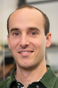
Research groups
Friedrich-Alexander University Erlangen-Nürnberg · Germany
ALD and electrochemical routes to structured thin films for energy conversion and storage.
Official profile & source
Research groups
Carleton University · Canada
Ligand and precursor design for ALD, with mechanistic studies of gas-phase and surface reactivity.
Official profile & source
ALD equipment
ALD systems & coating services
ALD systems for research and industrial applications, alongside thin-film coating services.
Official profile & source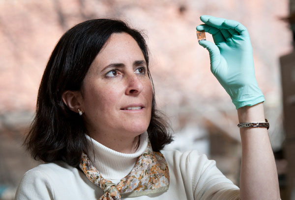
Research groups
Stanford University · USA
Surface chemistry and ALD mechanisms, area-selective deposition, and thin-film materials for electronics and energy.
Official profile & source
Metrology & characterization
Materials characterization
X-ray and atomic force microscopy tools for structure, surfaces and thin-film characterization.
Official profile & source
Research groups
Huazhong University of Science and Technology · China
Atomic-scale manufacturing centered on ALD: surface reactions, process development, equipment and applications in electronics, energy and catalysis.
Official profile & source
Simulation
Multiphysics modeling
Multiphysics simulation software for transport, fluid flow and chemical-reaction modeling.
Official profile & source
Simulation
Materials Studio
Materials Studio supports atomistic modeling of materials using quantum, classical and mesoscale methods.
Official profile & source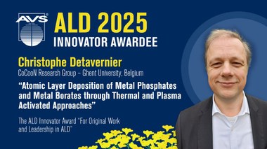
Research groups
Ghent University · Belgium
Conformal coatings of nanomaterials, with ALD growth, in situ characterization and applications in complex structures.
Official profile & source
Research groups
IFW Dresden / TU Dresden · Germany
Precursor chemistry and ALD/MOCVD processes for functional nanostructured materials in electronics and energy applications.
Official profile & source
Precursors & materials
Electronic materials & delivery
Electronic materials, precursor delivery and contamination-control products for semiconductor manufacturing.
Official profile & source
ALD equipment
Particle & wafer ALD
ALD equipment and surface-engineering technologies for particles and wafers.
Official profile & source
Research groups
University of Colorado Boulder · USA
Surface chemistry and nanoscale engineering through ALD, atomic layer etching and molecular layer deposition.
Official profile & source
Metrology & characterization
Scientific instrumentation
Ellipsometry, Raman spectroscopy and related instruments for materials and thin-film analysis.
Official profile & source
Metrology & characterization
Spectroscopic ellipsometry
Spectroscopic ellipsometers for thin-film thickness and optical-property characterization.
Official profile & source
Research groups
Aalto University · Finland
ALD and molecular layer deposition for functional inorganic and inorganic–organic thin-film materials.
Official profile & source
Research groups
Eindhoven University of Technology · Netherlands
Plasma-assisted ALD and atomic-scale processing, connecting plasma and surface science with functional thin films.
Official profile & source
Research groups
CIC nanoGUNE · Spain
Thin-film coating and material functionalization, including ALD and inorganic–organic hybrid nanomaterials.
Official profile & source
ALD equipment
Vacuum & deposition systems
Vacuum components, deposition systems and ALD technology for thin-film research.
Official profile & source
ALD equipment
Semiconductor wafer fabrication
Semiconductor process equipment spanning deposition, etch and atomic-scale processing.
Official profile & source
Research groups
Eindhoven University of Technology · Netherlands
Area-selective ALD and atomic-scale processing for nanoelectronics, with emphasis on reaction mechanisms and selectivity.
Official profile & source
Research groups
University of Oslo · Norway
ALD chemistry and functional thin-film materials, including oxides and hybrid materials.
Official profile & source
ALD equipment
Plasma Technology
Plasma-enhanced ALD systems and thin-film processing tools for research and device manufacturing.
Official profile & source
Research groups
North Carolina State University · USA
ALD thin-film growth and area-selective deposition for semiconductor materials and nanoscale processing.
Official profile & source
Research groups
Linköping University · Sweden
Chemistry of vapor deposition, including ALD and CVD routes for thin-film materials and conformal growth.
Official profile & source
Research groups
Humboldt University of Berlin · Germany
Functional nanostructures and thin-film materials, including ALD synthesis and coatings.
Official profile & source
Research groups
Aalto University · Finland
Catalysis and ALD surface chemistry, including conformality, porous materials and diffusion–reaction modeling.
Official profile & source
Research groups
University of Helsinki · Finland
Led by Mikko Ritala and Matti Putkonen, the group develops ALD chemistries, thin-film materials and reaction-mechanism studies.
Official profile & source
ALD equipment
Deposition & thin-film measurement
ALD and plasma processing systems, plus ellipsometry for thin-film characterization.
Official profile & source
ALD equipment
Semiconductor process equipment
Semiconductor deposition platforms including ALD within its thin-film process portfolio.
Official profile & source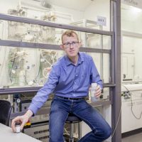
Research groups
Delft University of Technology · Netherlands
Particle technology and ALD on powders, connecting nanoscale coatings with scalable particle processing.
Official profile & source
Research groups
University of Colorado Boulder · USA
Particle ALD and functional coatings for energy, catalysis and materials processing.
Official profile & source
Research groups
Wayne State University · USA
Inorganic precursor chemistry and ALD processes for metal and metal-containing thin films.
Official profile & source
Research groups
University of California, Riverside · USA
Surface reactions relevant to ALD and catalysis, using molecular-level studies of thin-film growth and interfaces.
Official profile & sourceTry another keyword, category or initial letter.
Explore official websites for current publications, specifications and availability. This directory does not imply a partnership or endorsement. Portraits and logos identify their respective researchers and organizations.